-
Capability
-
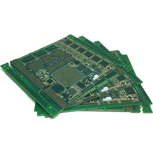
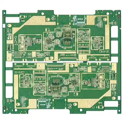
Multilayer PCB Capabilities
| ltem | Capability |
|---|---|
| Material | FR-4 Standard Tg 140°C, FR4-High Tg 170°C |
| Min. Track/Spacing | For External layers: 4oz Cu 10mil/13mil, 5oz Cu 12mil/15mil, 6oz Cu 15mil/15mil For Internal layers: 4oz Cu 8mil/8mil, 5oz Cu 10mil/10mil, 6oz Cu 12mil/12mil |
| Min. Hole Size | 0.15 ~ 0.3mm |
| Max Outer Layer Copper Weight (Finished) | 12oz |
| Max Inner Layer Copper Weight | 12oz |
| Board Thickness | 0.6-6mm |
| Surface Finishing | HASL lead-free, Immersion gold, OSP, Hard Gold, Immersion Silver, Enepig |
| Solder Mask | Green, Red, Yellow, Blue, White, Black, Purple, Matte Black, Matte green |
| Silkscreen | White, Black |
| Via Process | Tenting Vias, Plugged Vias, Vias not covered |
| Testing | Fly Probe Testing (Free) and A.O.I. testing |
| Build time | 5-15 days |
| Lead time | 2-3 days |
Introducing our multilayer PCB, designed to meet the increasing complexity and density requirements of modern electronic systems. Our multilayer PCBs offer enhanced functionality, improved signal integrity, and efficient use of space by incorporating multiple layers of conductive traces and insulating materials.
Our multilayer PCBs are suitable for a wide range of applications, including telecommunications, data storage, medical devices, aerospace, also consumer electronics, and more.
With their ability to accommodate high-speed signals, reduce electromagnetic interference, and provide design flexibility, our multilayer PCBs are the ideal choice for demanding electronic designs.
Key Features of Multilayer PCB:
- High Density and Space Optimization: Multilayer PCBs provide a higher level of component density and space optimization compared to single or double-sided PCBs. By stacking multiple layers of conductive traces and insulating materials, these PCBs allow for more compact designs, increased routing flexibility.
- Enhanced Signal Integrity: Multilayer PCBs offer improved signal integrity by providing dedicated signal layers and power/ground planes. The use of separate signal layers helps reduce crosstalk, noise, and electromagnetic interference (EMI), ensuring reliable signal transmission and also minimizing signal degradation in high-speed and high-frequency applications.
- Power Distribution and Grounding: Multilayer PCBs enable efficient power distribution and grounding. The inclusion of power and ground planes throughout the PCB ensures stable power supply and minimizes voltage drops. These planes also act as shielding layers, reducing electromagnetic emissions and enhancing system performance.
- Design Flexibility: Multilayer PCBs provide greater design flexibility compared to single or double-sided PCBs. They support complex circuitry, high-density component placement, and intricate routing patterns. This flexibility allows for the integration of advanced functionalities, such as high-speed interfaces, impedance matching, differential signaling, and RF/microwave circuitry.
- Reduced Electromagnetic Emissions: The use of dedicated ground and power planes in multilayer PCBs helps minimize electromagnetic emissions. This is crucial in applications where electromagnetic compatibility (EMC) is a concern, as it helps ensure compliance with regulatory standards and reduces the risk of interference with other electronic devices.
Frequently Asked Questions
1. How are Multilayer PCBs different from single-layer or double-layer PCBs?
2. What are the advantages of using Multilayer PCBs?
3. How are the layers in a Multilayer PCB connected?
4. What factors should be considered when designing a Multilayer PCB?
Why Choose Us
Extensive Proficiency
Benefiting from a wealth of 18 years in delivering exceptional box-build services, our profound expertise guarantees the highest quality in manufacturing our products.
Unyielding Dedication to Quality Assurance
Our collection of certifications serves as a testament to the remarkable quality of our offerings. Backed by certifications such as ISO 9001, ISO 13485, IPC-A-610, RoHS, and adherence to Lead-Free processes, we proudly hold registration and full REACH compliance, ensuring the utmost levels of quality.
Comprehensive Box Build Assembly
Embracing a holistic approach, NEWHONEST's box-build services offer extensive support throughout the entire mechanical assembly process. This encompasses a wide array of services, including component sourcing, innovative design, efficient manufacturing, meticulous testing, and comprehensive repair solutions.
Elevated Service Responsiveness
Harnessing the capabilities of cutting-edge automated SMT and lead-free wave soldering technologies, we emphasize our unwavering commitment to providing a responsive service that seamlessly extends from initial contact to the final delivery stage.