Medical Device PCB
The Medical device PCB Printed Circuit Board (PCB) business has expanded its irresistible beneficial influence due to the continuous growth of the tech world and its use in various fields. In recent years, its impact on the world of electronics has exceeded all forecasts, including IoT devices, smartphones, computers, artificial intelligence, and more.
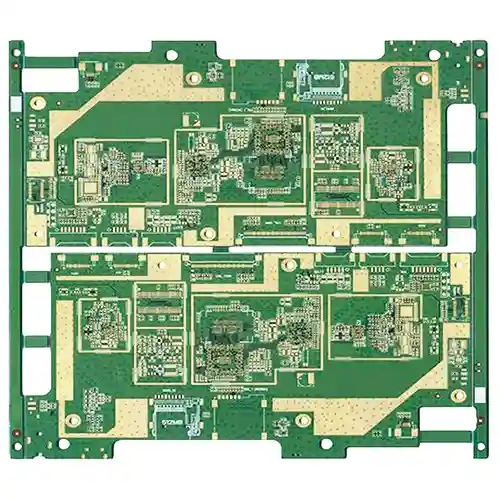
| Laminate | 8L |
| Dielectric constant | 4.2 |
| Plate Thickness | 1.6MM |
| Minimum Aperture: | 0.2mm |
| Minimum line width | 0.1MM |
| Minimum line spacing | 0.1MM |
Prototype to Full Turn-Key Assembly
Through-Hole Lead-Free Wave Soldering
Best Price, Genuine Components
Quality Accreditation ISO9001
-
Description
-
Specification
The use of Printed Circuit Boards (PCBs) in medical devices has greatly expanded due to technological advancements. These boards are crucial in various areas like smartphones, computers, and medical gadgets. They are now transforming healthcare by connecting patients and doctors through advanced medical technology.
PCBs help create convenient medical devices that address healthcare challenges, such as accurate diagnoses and patient monitoring. The medical electronics industry is rapidly growing, with the global market predicted to reach $4.4 billion by 2022. As technology advances, PCBs become increasingly essential in medical devices due to their digital nature.
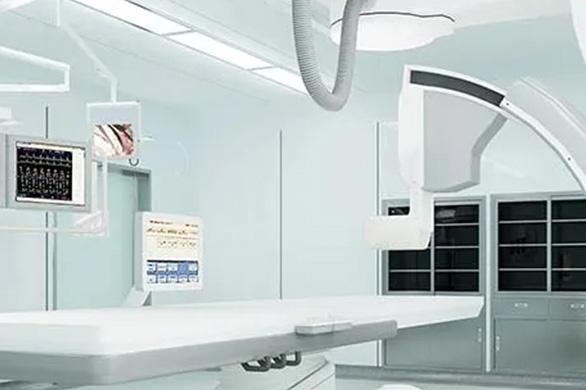
Medical devices like defibrillators, MRI machines, and ultrasound equipment rely on PCBs to function properly. Special care is needed when making medical PCBs, especially for implants. High-Density Interconnect (HDI) PCBs, which have components tightly packed, are commonly used.
Several techniques are employed in medical PCB assembly:
- HDI / via-in-pad technology: This involves placing vias (holes) inside copper pads to save space on the PCB. It allows for more component placement and smaller electronics.
- Surface Mount Technology (SMT): SMT is used in most devices as it allows for smaller components, automated assembly, and cost savings.
- PCB fine lines and spaces: This technology, with tiny lines and spaces, is important for compact devices, enhanced wiring, and cost-effective manufacturing.
PCBs are used in various medical applications:
- Scanning equipment: CT scanners, X-ray machines, and ultrasound devices rely on electronic components.
- Monitors: Heart rate monitors, blood glucose monitors, and blood pressure monitors incorporate electronic parts.
- Medical Instruments: Instruments for data collection and testing, like electron microscopes and control systems, contain PCBs.
Health standards and reliability are crucial in the medical industry. Medical device PCBs are designed smaller to fit in devices. This technology’s growth in healthcare is opening new opportunities for innovation.
| Feature | Capability |
|---|---|
| Material | FR-4 Standard Tg 140°C, FR4-High Tg 170°C |
| Min. Track/Spacing | For External layers: 4oz Cu 10mil/13mil, 5oz Cu 12mil/15mil, 6oz Cu 15mil/15mil For Internal layers: 4oz Cu 8mil/8mil, 5oz Cu 10mil/10mil, 6oz Cu 12mil/12mil |
| Min. Hole Size | 0.15 ~ 0.3mm |
| Max Outer Layer Copper Weight (Finished) | 12oz |
| Max Inner Layer Copper Weight | 12oz |
| Board Thickness | 0.6-6mm |
| Surface Finishing | HASL lead-free, Immersion gold, OSP, Hard Gold, Immersion Silver, Enepig |
| Solder Mask | Green, Red, Yellow, Blue, White, Black, Purple, Matte Black, Matte green |
| Silkscreen | White, Black |
| Via Process | Tenting Vias, Plugged Vias, Vias not covered |
| Testing | Fly Probe Testing (Free) and A.O.I. testing |
| Build time | 5-15 days |
| Lead time | 2-3 days |