-
Capability
-
12 Layer PCB Stackup Capability
| ltem | Capability |
|---|---|
| Quality Grade | Standard IPC 2 and IPC 3 |
| Number of Layers | 2 – 40layers |
| Order Quantity | 1pc – 1Million+pcs |
| Build Time | 24H – 4weeks |
| Material | S1150G, S1165, S1000-2 |
| Board Size | Min 5*5mm | Max 500*650mm |
| Board Thickness | 0.4mm – 6.5mm |
| Copper Weight (Finished) | 0.5oz – 10.0oz |
| Min Tracing/Spacing | 3mil/3mil |
| Solder Mask Sides | As per the file |
| Solder Mask Color | Green, White, Blue, Black, Red, Yellow |
| Silkscreen Sides | As per the file |
| Solder Mask Color | White, Black, Yellow |
| Min Annular Ring | 4mil |
| Min Drilling Hole Diameter | 6mil |
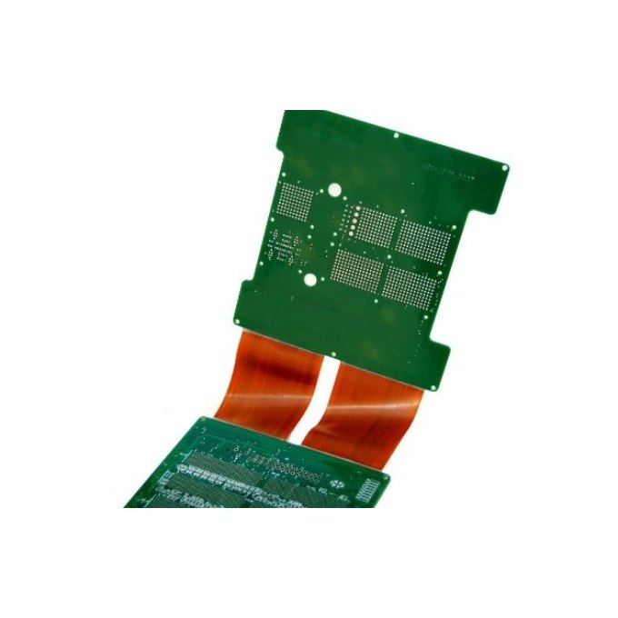
12-Layer PCB Stackup: Superior Multilayer Circuitry
The 12-Layer PCB Stackup offered by us presents a remarkable solution for intricate electronic designs requiring advanced functionality. With a total of twelve layers meticulously arranged, this multilayer circuit board provides exceptional capabilities for complex applications.
Key Features:
- Layer Diversity: Our 12-layer stackup facilitates intricate designs by allowing multiple layers of conductive pathways, providing ample space for routing signals and power distribution.
- Enhanced Signal Integrity: The carefully engineered layer arrangement minimizes signal interference, ensuring optimal signal integrity even in high-frequency applications.
- Power Distribution Efficiency: With dedicated power and ground planes, this stackup optimizes power distribution, reducing noise and ensuring stable performance.
- High-Density Components: The 12-layer stackup accommodates densely packed components, enabling the creation of compact and efficient electronic systems.
- EMI Shielding: The multiple layers aid in electromagnetic interference (EMI) shielding, enhancing the overall electromagnetic compatibility of the PCB.
- Advanced Applications: Ideal for applications demanding intricate circuitry, such as advanced communication systems, high-speed data transfer, and complex industrial control systems.
- Reliability: Crafted with precision and manufactured under stringent quality control, our 12-layer PCB stackup is designed to meet the demands of mission-critical applications.
Whether it’s the intricacies of high-speed data transmission or the demands of advanced industrial automation, our 12-layer PCB stackup offers the foundation for innovative electronic solutions. With our commitment to excellence and cutting-edge manufacturing processes, you can trust in the reliability and performance of our multilayer circuit boards
Frequently Asked Questions
Highlighting the differences between OEM PCBs and standard PCBs.
What does Wenshu's approach entail when it comes to PCB design?
How does Wenshu PCB design go about guaranteeing product reliability and quality?
What procedures are adopted to ensure confidentiality during the manufacturing of Wenshu PCBs?
Why Choose Us
Enhanced Service Responsiveness
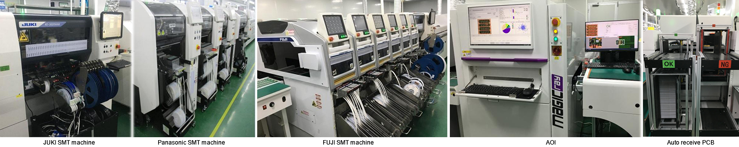
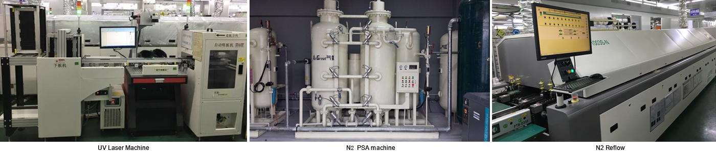
Capitalizing on cutting-edge automated SMT and lead-free wave soldering technologies, our focus revolves around delivering a swift and responsive service that seamlessly spans from initial engagement to final delivery phases.
Thorough Box Build Assembly
NEWHONEST's box build services encompass a comprehensive methodology, providing thorough support throughout the mechanical assembly journey. This encompasses a range of services, including component sourcing, design, manufacturing, rigorous testing, and comprehensive repair solutions.
Uncompromised Quality Assurance
Our collection of certifications serves as a testament to the outstanding quality of our offerings. With ISO 9001, ISO 13485, IPC-A-610, RoHS, and Lead-Free process certifications, our commitment extends beyond mere registration to complete REACH compliance, ensuring the utmost quality.
Years of Experience
With a rich history of 18 years in providing top-notch box-build services, our deep knowledge ensures the best quality in making our products.