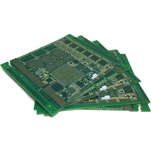
14-Layer PCB Circuit Board
A 14-layer PCB circuit board stackup can be referred to as a multi-layer printed circuit board device, and it must be used whenever you need 8 signal layers. In addition to that, when you need a special shield made of net, a 14-layer pcb stackup will be required.
| Layers | 14L |
| Panel size | 120*95mm/1 |
| Plate Thickness | 2.4mm |
| Minimum through hole | 0.20mm |
| Minimum BGA | 0.25mm |
| Line width line spacing | 3/3.2mil |
Prototype to Full Turn-Key Assembly
Through-Hole Lead-Free Wave Soldering
Best Price, Genuine Components
Quality Accreditation ISO9001
-
Description
-
Specification
A 14-layer PCB circuit board stackup is like a versatile puzzle made of layers that are used in many different things like satellite dishes, preamplifiers, memory modules, and more. Think of it as a special board that’s really helpful when you need to connect 8 signal layers together. It’s also great when you want to create a special shield using a net.
Applications
Here are some places where a 14-layer PCB stackup is used:
Industries: Industries use the 14-layer PCB stackup for things like control systems and industrial computers. These boards are also handy in manufacturing to operate machines because they’re small, strong, and can handle a lot.
Electronics: You know things like microwave ovens and smartphones? They use circuit boards to work, and nowadays, many of them use the 14-layer PCB stackup instead of the usual kind because it’s better.
Cars: Even cars use the 14-layer PCB stackup! Things like the headlight switch, GPS, and engine sensors all need it. Electric cars use it too for different parts.
Medical Stuff: In hospitals and medical places, lots of machines like X-ray machines and heart monitors use the 14-layer PCB stackup to do their jobs well.
Phones and Communication: Phones and things used to talk to each other also use the 14-layer PCB stackup. It helps with stuff like GPS, signals, and satellites. It’s used in those big tower things and mobile devices too.
Benefits
Now, why is the 14-layer PCB stackup so good? Well, there are some reasons:
Great Quality: Making a 14-layer PCB stackup takes a lot of careful planning. That’s why it’s high quality and trustworthy compared to other types. You can rely on it.
Small and Handy: This type of PCB is smaller than others with the same abilities. It’s like a sandwich of layers, so it’s really compact. This makes it awesome for modern technology.
Super Powered: The 14-layer PCB stackup packs lots of layers into one board. This is why it’s super fast and powerful.
Tough and Strong: It can handle tough situations with heat and pressure. The layers are connected really well, and they can stand up to challenges. This makes the 14-layer PCB stackup really strong.
Bends and Shapes: It’s also flexible! The way it’s made lets it bend a bit, which is handy in situations where things need to flex a little.
| Feature | Capability |
|---|---|
| Material | FR-4 Standard Tg 140°C, FR4-High Tg 170°C |
| Min. Track/Spacing | For External layers: 4oz Cu 10mil/13mil, 5oz Cu 12mil/15mil, 6oz Cu 15mil/15mil For Internal layers: 4oz Cu 8mil/8mil, 5oz Cu 10mil/10mil, 6oz Cu 12mil/12mil |
| Min. Hole Size | 0.15 ~ 0.3mm |
| Max Outer Layer Copper Weight (Finished) | 12oz |
| Max Inner Layer Copper Weight | 12oz |
| Board Thickness | 0.6-6mm |
| Surface Finishing | HASL lead-free, Immersion gold, OSP, Hard Gold, Immersion Silver, Enepig |
| Solder Mask | Green, Red, Yellow, Blue, White, Black, Purple, Matte Black, Matte green |
| Silkscreen | White, Black |
| Via Process | Tenting Vias, Plugged Vias, Vias not covered |
| Testing | Fly Probe Testing (Free) and A.O.I. testing |
| Build time | 5-15 days |
| Lead time | 2-3 days |