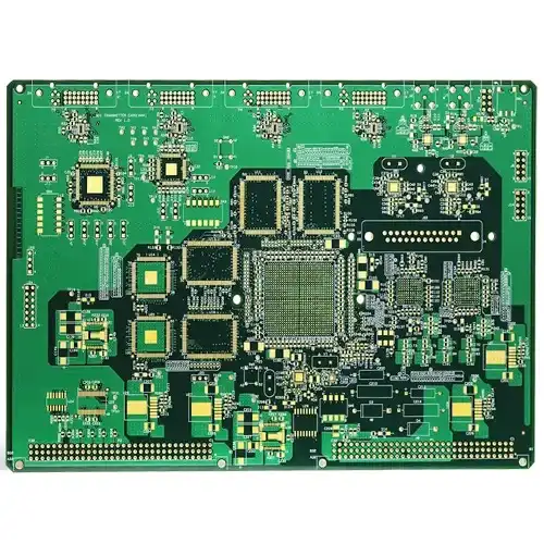
10-Layer 1-Stage HDI Communication PCB
The 10-Layer 1-Stage HDI Communication PCB is an advanced printed circuit board designed specifically for communication applications that require high-density interconnect (HDI) technology. It offers superior signal integrity, increased functionality, and enhanced reliability. This also makes it well-suited for use in telecommunications, networking, and other communication systems.
| Plate thickness | 1.2mm |
| Panel Size | 110.8*94.8mm/4 |
| Minimum blind hole | 0.10mm |
| Minimum BGA | 0.20mm |
| Minimum through hole | 0.20mm |
| Line width and line spacing | 2.5/2.2mil |
Prototype to Full Turn-Key Assembly
Through-Hole Lead-Free Wave Soldering
Best Price, Genuine Components
Quality Accreditation ISO9001
-
Description
-
Specification
Introducing the 10-Layer 1-Stage HDI Communication PCB – an innovation tailored to revolutionize communication applications with its cutting-edge design. Engineered to perfection, this advanced printed circuit board stands as a pinnacle of High-Density Interconnect (HDI) technology, setting new standards in signal integrity, functionality, and reliability. Crafted to excel in the demands of telecommunications, networking, and diverse communication systems, this PCB ensures seamless and efficient data transmission.
Technical Excellence:
With meticulously engineered features, the 10-layer 1-Stage HDI Communication PCB boasts unparalleled technical prowess. It embraces a spectrum of impedance options, including 50 Ω for antennas and 90Ω & 100Ω for differential impedance, empowering your communication devices to transmit data with remarkable accuracy and speed. These impedance configurations ensure consistent and stable signal propagation, mitigating the risks of data loss and distortion.
Versatility Redefined:
This PCB’s applications are as diverse as they are impactful. From the sleek lines of cell phones and tablets to the sophisticated precision of ultrabooks and E-readers, the 10-Layer 1-Stage HDI Communication PCB integrates seamlessly into various devices. This PCB has become an indispensable foundation for the modern technological landscape, with compatibility extending to MP3 players, GPS units, portable game consoles, digital cameras, LCD TVs, and POS terminals.
Performance Amplified:
Experience a leap forward in electronic performance. By leveraging HDI technology, this PCB effectively reduces product weight and overall dimensions while drastically enhancing the electrical capabilities of the end product. This remarkable feat paves the way for devices that are compact, efficient, and powerful in their performance, setting a new benchmark for electronic innovation.
Limitless Possibilities:
From medical equipment to electronic aviation components, the 10-layer 1-Stage HDI Communication PCB is applied in an expansive spectrum of industries. Its adaptability and versatility make it a cornerstone of modern electronic design. As the world continues to push the boundaries of what’s possible, this PCB remains at the forefront of technological evolution, unlocking new dimensions of connectivity and communication.
In a world of paramount seamless communication, the 10-layer 1-Stage HDI Communication PCB rises with unmatched precision and reliability. Redefine what’s achievable in electronic interconnectivity – choose innovation that makes a difference.
| Feature | Capability |
|---|---|
| Material | FR-4 Standard Tg 140°C, FR4-High Tg 170°C |
| Min. Track/Spacing | For External layers: 4oz Cu 10mil/13mil, 5oz Cu 12mil/15mil, 6oz Cu 15mil/15mil For Internal layers: 4oz Cu 8mil/8mil, 5oz Cu 10mil/10mil, 6oz Cu 12mil/12mil |
| Min. Hole Size | 0.15 ~ 0.3mm |
| Max Outer Layer Copper Weight (Finished) | 12oz |
| Max Inner Layer Copper Weight | 12oz |
| Board Thickness | 0.6-6mm |
| Surface Finishing | HASL lead-free, Immersion gold, OSP, Hard Gold, Immersion Silver, Enepig |
| Solder Mask | Green, Red, Yellow, Blue, White, Black, Purple, Matte Black, Matte green |
| Silkscreen | White, Black |
| Via Process | Tenting Vias, Plugged Vias, Vias not covered |
| Testing | Fly Probe Testing (Free) and A.O.I. testing |
| Build time | 5-15 days |
| Lead time | 2-3 days |