Guide to Common PCB Issues & Failures
Printed circuit boards (PCB) are essential components of many electrical devices today, connecting different components to one another through a complex array of circuits. Global demand for PCBs has risen rapidly — over the past eight years, total global sales of printed circuit boards have increased by an average of over $3.7 billion per year, with an increased focus on reducing conflict mineral supply chain issues and improving the technology. Worldwide sales of PCBs stood at about $82 billion as of 2018.
With so much money invested in PCBs and the role they play in numerous electrical devices and box build assemblies, PCB failure is a major concern of many companies. Below, you’ll learn more about the most common reasons behind PCB failure to put your company in a better position to prevent and address PCB failure effectively.
WHAT IS PCB FAILURE?
PCB failure can occur for several reasons, with the end result being that the PCB no longer functions properly. Since PCBs are used in many electronics, such as wearables, airplanes, satellites and medical devices, it’s crucial that any failures are identified quickly and the appropriate action is taken. Any company looking to keep their electronics running smoothly can better address PCB failure and even prevent it from occurring by knowing more about why it happens.
REASONS FOR PCB FAILURE – PCB DEFECTS
The complexity of the PCB design and manufacturing processes means there are numerous opportunities for PCB failure issues to arise. Some of these failures are a result of design oversights, such as insufficient clearances or incorrect measurements, which can negatively affect the functionality of the finished product. Others may result from problems in the manufacturing process, such as drilling errors or over-etching, which can be equally catastrophic.
Fortunately, most of these errors can be avoided with knowledge and consideration for the manufacturing process, as well as awareness of the more common PCB manufacturing issues. Following a set of standard design rules and considerations can aid in preventing component failure, connection issues and other circuit board problems. To help you and your company better understand and avoid the potential errors in your printed circuit board designs, we’ve compiled a list of the most common issues experienced in PCB manufacturing, why they occur and how they can be prevented below:
1. PLATING VOIDS
Plated through-holes are copper-coated holes in a printed circuit board. These holes allow electricity to be carried from one side of the circuit board to the other. To create these holes, the PCB board fabricator drills holes through the circuit board, puncturing the base material all the way through. A layer of copper foil or a copper coating is then added to the surface of the material and along the walls of these holes through an electroplating process.
This process deposits a thin layer of electroless copper onto the circuit board in a process called deposition. After this step, extra layers of copper are added and etched to create the circuit image.
While effective, the deposition process is not perfect and can result in voids in the plating under certain circumstances. Plating voids are effectively gaps or holes in the plating of the circuit board and are usually the result of problems during the deposition process. These plating voids are particularly problematic because imperfections in the plating of a thru-hole prevent an electrical current from passing through the hole, resulting in a defective product.
These plating voids happen because, for one reason or another, the material does not coat evenly during the deposition process. The reasons for this include contamination of the material, air bubbles caught in the material, insufficient cleaning of the holes, insufficient catalyzation of the copper in the deposition process or rough hole drilling. Any of these problems can result in plating voids along the walls of the circuit holes.
Defects as a result of contamination, air bubbles or insufficient cleaning can be avoided by cleaning the material properly after drilling. Additionally, PCB defects from faulty drilling can be avoided by closely following the manufacturer’s directions during use, such as the recommended number of drill hits, drill in-feeds and drill speeds. Both problems can be avoided by hiring a well-qualified and experienced PCB manufacturing company.
2. INSUFFICIENT COPPER-TO-EDGE CLEARANCE
Copper is an incredibly conductive metal, which is used as an active component of PCBs. However, copper is also relatively soft and vulnerable to corrosion. To prevent corrosion and protect the copper from interacting with its environment, this copper is covered with other materials. However, when a PCB is trimmed, if the copper is too close to the edge, part of this coating can be trimmed as well, exposing the copper layer underneath. This can cause numerous problems in the functionality of the board.
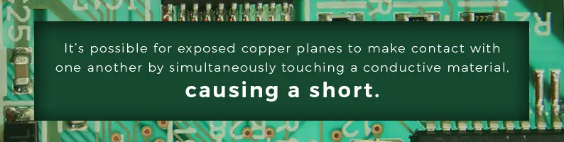
For one, it is possible for the exposed copper planes to make contact with one another by simultaneously touching a conductive material, causing a short. This exposure also leaves the copper open to the environment, making it vulnerable to corrosion. This exposure also increases the chance of someone contacting the PCB and receiving an electrical shock. In addition, poorly insulated copper tracks are more prone to plating voids.
This problem can easily be avoided by making sure the space between the edge of the copper and the edge of the board, also known as the copper-to-edge or plate-to-edge clearance, follows acceptable standards for the type of board being manufactured. A thorough Design for Manufacturability (DFM) check by your manufacturer will usually catch any potential problems.
3. BAD SOLDERING
Improper soldering during the printed circuit boa assembly process can lead to major issues. One of the most common kinds of poor soldering occurs when a technician doesn’t heat the solder enough, leading to cold soldering, which can cause PCB failure. Additionally, moisture during the soldering process can contaminate the PCB pad and other components. This contamination can cause PCB components to burn and create connection problems. Companies often use visual or X-ray inspections to detect bad soldering.
4. SLIVERS
Slivers are narrow wedges of copper or solder mask produced during the PCB manufacturing process and can cause serious problems during the fabrication of circuit boards. These slivers are often produced during the etching process and can occur in one of two ways.
First, slivers can be produced when an extremely long, thin feature of the copper or solder mask is etched away. In some cases, this sliver detaches before it fully dissolves. These detached slivers can float around in the chemical bath, and can potentially land on another board, adding an unintended connection.
Another way to produce slivers is to cut a section of the PCB design too narrowly or too deeply. Even if they are intended to stay attached to the board, if an etched section is narrow enough or the etching is deep enough, a sliver of material can completely or partially detach, either producing a floating sliver or a peeled-back sliver. Both of these options can have serious negative consequences for the circuit board’s function.
These slivers can either connect to other pieces of copper or expose copper plating that would normally be covered by the solder mask. The former problem can cause a short, therefore producing a defective circuit board, while the latter option can result in corrosion of the copper over time. Both of these problems reduce the lifespan of the circuit board.
Slivers can be avoided by designing sections with minimum widths, reducing the chances of producing slivers. A manufacturer will usually spot potential slivers with a DFM check.
5. MISSING SOLDER MASK BETWEEN PADS
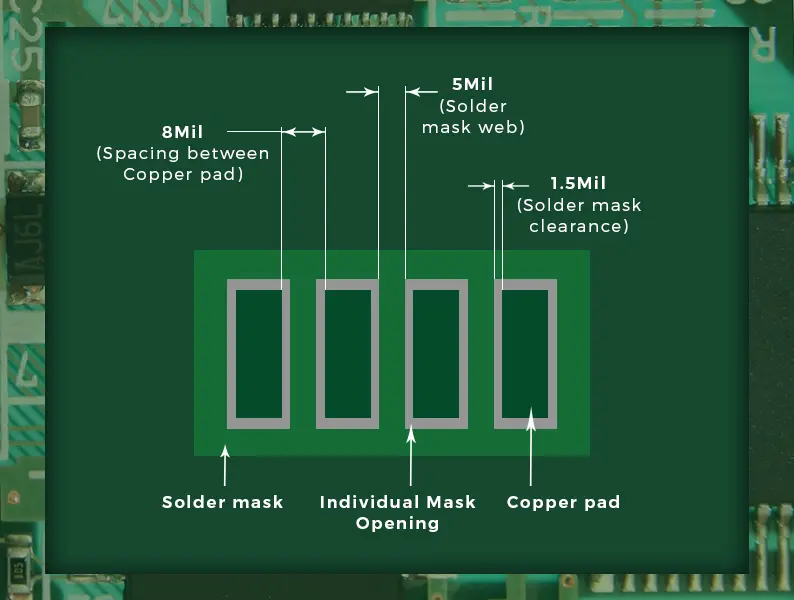
The solder mask is the layer on top of the circuit board’s copper layer. This solder mask is laid on top of the copper layer to insulate the copper traces from accidental contact with other metal, solder or conductive bits. It also acts as a barrier between the copper and the environment, preventing corrosion and protecting the circuit board’s handlers from electrocution. Pads are the portions of metal left exposed by the solder board, which components are soldered to.
In some circuit boards, the solder mask may be partially or completely absent between pads. This exposes more copper than is necessary and can result in solder bridges forming accidentally between pins during the assembly process. This can result in a short, as well as reduced corrosion protection, both of which can negatively affect the functionality and longevity of the circuit board.
This defect is commonly due to a design oversight, where the solder mask is undefined or the settings for a larger board are carried over to a smaller board, resulting in pad holes that are simply too large for the smaller PCB. This can be avoided by double-checking the design before sending it to the manufacturer.
However, oversights do happen, so make sure you have a good manufacturer with a proper DFM check protocol since these manufacturers can catch such issues before they become a real problem.
6. ACID TRAPS
“Acid trap” is the common term for acute angles in a circuit. They are referred to this way because these acute angles trap acid during the PCB etching process, allowing the acid to build up in the nook of the angle. The angle functionally keeps the acid in the corner for a longer period than the design calls for, causing the acid to eat away more than intended. As a result, the acid can compromise a connection, making the circuit defective and causing more serious problems later on.
Most designers are aware of the problems caused by acute angles in a circuit board and are therefore trained to avoid them. However, mistakes do happen. Often, PCB acid traps are the result of simple human error, although some design software programs may also set circuits to acute angles if the settings are not properly adjusted.
Most designers will catch acute angles as they double-check their work, though oversights are possible. If this is the case, a good manufacturer will catch these mistakes with a DFM check. Get Pricing and Lead Time
7. POORLY MANUFACTURED COMPONENTS
Another cause of PCB failure occurs when an engineering team uses poorly manufactured components. During PCB production, physical damage due to improper components used during electronic assembly can harm the PCB and cause power failure. Common PCB assembly defects and faults from poorly manufactured components include connection issues and loose parts.
Additionally, residual flux, a substance used during soldering, left on a PCB panel can do major damage and can lead to the need for circuit board repairs. Successful companies ensure they’re working with manufacturers that use high-quality components in their PCBs.
8. STARVED THERMALS
Thermals are small traces surrounding pads and are used to connect pads to the plane. These thermals allow the pads to more effectively disperse heat, and are important components during the soldering process. Sometimes, however, voids between the thermal and the rest of the plane, or the thermal and the pad, can result in an incomplete connection, reducing the effectiveness of the heat transfer system these thermals create. This can result in several functional problems.
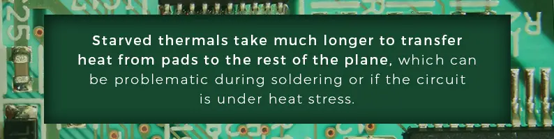
Starved thermals take much longer to transfer heat from pads to the rest of the plane, which can be problematic during soldering or if the circuit is under heat stress. A thermal pad with improper heat transfer may solder oddly and will take an abnormally long time to reflow, slowing down the assembly process. After manufacturing, circuit boards with starved thermals may suffer from insufficient heat transfer and may be more prone to overheating and heat damage.
The source of overheating and heat damage is most often found in the manufacturing process. These thermal connections are usually tied correctly to a plane layer in a computer-aided design (CAD) system but are somehow manufactured with a reduced connection to the rest of the plane. Manufacturing problems during thermal molding or machining, such as over-machining or improper molding, can all result in this issue. To remedy this issue, it’s usually best practice to replace the thermal.
An experienced and highly rated manufacturing company can identify such faulty thermals easily and replace them before they have a chance to cause problems in the circuit board.