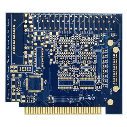
Double-Sided Gold Finger Circuit Board
Gold fingers are the gold-plated posts you see on the edge of a printed circuit board (PCB) connection. The purpose of the golden finger is to connect the auxiliary PCB to the motherboard of the computer. PCB gold fingers are also used in various other devices that communicate via digital signals, such as consumer smartphones. Gold is used for connection points along the PCB due to the alloy’s excellent electrical conductivity.
| Layers | 2L |
| Plate thickness | 1.6mm |
| Minimum aperture | 0.3mm |
| Line width | 0.15mm |
| Line distance | 0.15mm |
| Surface Treatment | Immersion Gold |
Prototype to Full Turn-Key Assembly
Through-Hole Lead-Free Wave Soldering
Best Price, Genuine Components
Quality Accreditation ISO9001
-
Description
-
Specification
Presenting the Double-Sided Gold Finger Circuit Board – an engineering marvel designed to seamlessly connect and empower various devices through the language of digital signals. A fusion of technology and craftsmanship, this circuit board is at the forefront of modern connectivity solutions, enhancing the reliability and efficiency of your electronics.
Key Features:
- Efficient Connectivity: Gold finger PCBs come adorned with gold-plated finger-like pads that facilitate robust connections, often used as edge connectors. These gold fingers allow efficient communication between circuit boards, enabling seamless data transfer.
- Two Gold Options: Two types of gold are suitable for gold finger plating. Electroless Nickel Immersion Gold (ENIG) is cost-effective and easy to solder but better suited for non-frequent insertion. Electroplated hard gold is sturdy, thick (around 30u”), and ideal for frequent usage.
- Enhanced Durability: The electroplated hard gold offers remarkable durability, making it perfect for repeated insertions and ejections without wearing out the contacts. This robust nature ensures sustained connectivity over time.
- Precise Insertion: Gold fingers are often chamfered or beveled to ensure effortless insertion. These bevel cuts can be tailored to specific requirements, ensuring easy connections without hassle.
- Visual and Tape Testing: Rigorous quality checks are conducted to ensure the integrity of gold finger plating. Visual inspections ensure a clean, smooth surface with no unwanted plating. Tape tests verify plating adhesion by assessing if the plating adheres firmly to the contacts.
- Standardized Production: The Connected Electronics Industry Association (IPC) established production standards for PCB gold fingers. These standards, refined over time, focus on aspects like composition, thickness, and adhesion quality.
Benefits:
- Dependable Connectivity: Gold finger PCBs are vital for seamless communication between devices and equipment, ensuring commands are executed flawlessly.
- Longevity: The durable nature of gold-plated connections allows frequent insertions and ejections without the fear of wearing down, guaranteeing sustained connectivity.
- Electrical Conductivity: Gold’s exceptional electrical conductivity ensures efficient data transfer, minimizing signal loss and ensuring accurate communication.
- Corrosion Resistance: The corrosion-resistant nature of gold further solidifies its role as a reliable connector, ensuring consistent performance even in challenging environments.
- Industry Compliance: The production standards set by IPC ensure that gold finger PCBs adhere to rigorous quality checks, maintaining high levels of reliability and performance.
Embrace the power of gold in connectivity with the Double-Sided Gold Finger Circuit Board. Its precision-plated contacts ensure unswerving performance, facilitating the fluid exchange of information in your electronic devices. Trust in the reliability of gold to bridge the gap between devices, ensuring a world of uninterrupted communication.
| ltem | Capability |
|---|---|
| Layer Count | 1-40layers |
| Base Material | KB、Shengyi、ShengyiSF305、FR408、FR408HR、IS410、FR406、GETEK、370HR、IT180A、Rogers4350、Rogers4000、PTFE Laminates(Rogers series、Taconic series、Arlon series、Nelco series)、Rogers/Taconic/Arlon/Nelco laminate with FR-4 material (including partial Ro4350B hybrid laminating with FR-4) |
| Board Type | Backplane、HDI、High multi-layer blind&buried PCB、Embedded Capacitance、Embedded resistance board 、Heavy copper power PCB、Backdrill, PCB Gold Finger |
| Board Thickness | 0.2-5.0mm |
| Copper Thickness | Min. 1/2 OZ, Max. 10 OZ |
| PTH Wall | 25um(1mil) |
| Maximum Board Size | 1100*500mm(43”*19”) |
| Min laser drilling size | 4mil |
| Min.spacing/Tracing | 2.7mil/2.7mil |
| Solder Mask | Green, Black, Blue, Red, White, Yellow, Purple matte/glossy |
| Surface Treatment | Flash gold(electroplated gold)、ENIG、Hard gold、Flash gold、HASL Lead-free 、OSP、ENEPIG、Soft gold、Immersion silver、Immersion Tin、ENIG+OSP, ENIG+Gold finger, Flash gold(electroplated gold)+Gold finger(50u”), Immersion silver+Gold finger, Immersion Tin+Gold finger |
| Min. Annular Ring | 3mil |
| Aspect ratio | 10:1(HASL Lead-free 、HASL Lead、ENIG、Immersion Tin、Immersion silver、ENEPIG);8:1(OSP) |
| Impedance control | ±5ohm(<50ohm), ±10%(≥50ohm) |
| Other Techniques | Blind/Buried Via, Gold Fingers, Press Fit, Via in Pad, Electrical Test |